

Power Semiconductors
IGBT
High-speed switching performance and high-voltage capabilities
An IGBT (Insulated Gate Bipolar Transistor) is a semiconductor device that combines the high-speed switching performance of a power MOSFET with the high-voltage/high-current capabilities of a bipolar transistor. Fuji Electric’s IGBT modules are designed for use as switching elements for power converters of variable speed drives for motors, uninterruptable power supplies and others.
Explore our new 8th-Generation technology ↓
Products


Features of IGBT module A Series
1. Development of 8th-Generation Devices
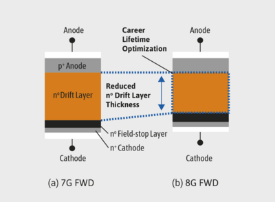
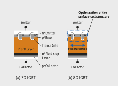
To improve VCE(sat) and turn-on loss (Eon), new 8G IGBT and FWD devices have been developed. The below figures show cross-sectional views comparing the 1,200V 8G IGBT/ FWD devices with the 7G devices. In the IGBT, the surface cell structure is miniaturized to increase the accumulated carrier density in the drift layer, lowering conduction losses. The arrangement pattern of this surface cell structure is further optimized to reduce Eon. For the FWD, the drift layer has been thinned, and the carrier lifetime has been precisely controlled to optimize carrier distribution, effectively reducing the reverse recovery loss (Err).
2. Packaging Technology and Reliability Enhancements
To ensure long-term reliability and stable high-temperature operation, the solder beneath the insulating substrate was improved. Conventional solder can crack under repeated thermal stress, increasing thermal resistance and causing overheating. As a result, the maximum case temperature (Tc) was limited to 125°C. To overcome this limitation, a newly developed high-strength solder material was adopted.
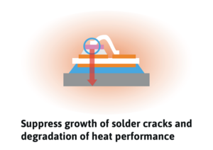
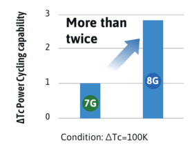
By optimizing key physical properties such as melting point, creep behavior, and thermal expansion, the new solder significantly reduces crack formation caused by thermal stress and maintains stable thermal performance over time. As shown in the figure on the right, the ΔTc power cycling capability is more than twice that of the conventional design, improving operating margin, thermal management flexibility, and reducing maintenance costs.
3. Low Power Dissipation
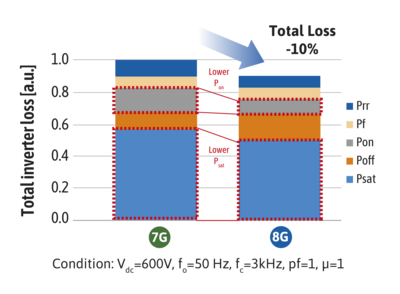
The module has been optimized by reducing the thickness and miniaturizing the structure of the IGBT chip and diode chip that make up the module. This reduces power losses during inverter operation compared to the previous 7th generation X series. The figure below shows the calculated losses of the 8G module under typical inverter conditions. Reduced conduction loss (Psat), turn-on loss (Pon), and reverse recovery loss (Prr) lead to a 10% total inverter loss reduction compared to 7G.Although the turn-off loss (Poff) slightly increases, the device was intentionally optimized for lower VCE(sat) to minimize overall inverter loss under practical conditions. As a result, the total inverter loss is still reduced.In addition, the 10% loss reduction, together with the higher Tc limit enabled by the new solder material, allows higher output current before reaching the Tvj limit of 175°C.
Get in contact
Our experts will answer any further questions you have about Fuji Electric and our technologies.